Privacy statement: Your privacy is very important to Us. Our company promises not to disclose your personal information to any external company with out your explicit permission.
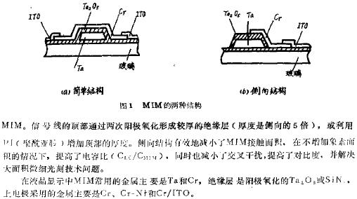
MIM is a sandwich structure composed of a metal, insulator, and metal three-layer film. The MIM structure for liquid crystal display is shown in Figure 1. There are two main types: (1) Figure 1 (a) is a relatively common "T" structure. The process of this structure is relatively simple, and the MIM developed in the early stage is basically this form. However, the MIM area of this structure is relatively large, and has a large parasitic capacitance, which is disadvantageous for improving contrast and improving display quality. If you want to reduce the area, you need a large area, high resolution lithography equipment. Not only does it increase the difficulty of the production process, the yield rate decreases, but also increases the cost, and is not suitable for large-scale display. (2) Figure 1 (b) shows the lateral MIM structure developed, which is formed laterally on the scan line.
This article refers to the address: http://

MIM decisive action
The M IM component is characterized by a non-linear change in its volt-ampere characteristics. LCD display is the use of this feature of MIM. When the applied bias voltage reaches a certain value V (closed voltage), the electrical conductivity of the MIM changes abruptly and rapidly changes from the insulated state to the conductor state. The current through the MIM also increases rapidly. MIM is in the "on" state. When the applied bias voltage on the MIM is less than VT, the MIM returns to its original state and the MIM is in the "lizard" state. The insulation properties of the insulation are not damaged throughout the "pass," "lizard" process. Figure 2 shows the volt-ampere characteristic of MrM.

MIMI communication mechanism
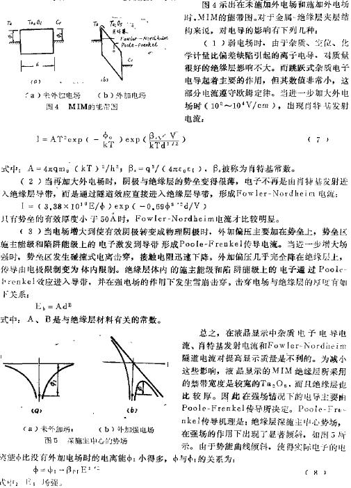
Therefore, under the action of a strong field, a large amount of electrons on the donor level enter the insulating layer conduction band. And avalanche breakdown occurs under the action of a strong field. The relationship between its volt-ampere characteristics can be expressed by the formula (1). For the MIM whose insulating layer is Ta zO, the 13 PF value of the MIM obtained in the actual work does not conform to the PooIe-Frenkel3L~ argument and conforms to Schottky's theoretical value s (13 PF).
=2 13 s). The appearance of this abnormal Poole-Frenke1 effect is mainly due to the existence of only neutral trap levels in the Ta zO film, so the Poole-F reakel effect cannot be exhibited. In this case, the conductivity is also low. In order to solve this problem, a deep donor level must be formed in the Ta:O film by a heat treatment process to meet the requirements of the liquid crystal display. Part of the non-equilibrium defects can also be removed during the process to improve the stability of the MIM.

Author:
Ms. vicky
Phone/WhatsApp:
+8613777096783
이 업체에게 이메일로 보내기
Author:
Ms. vicky
Phone/WhatsApp:
+8613777096783
January 29, 2022
December 18, 2021

Privacy statement: Your privacy is very important to Us. Our company promises not to disclose your personal information to any external company with out your explicit permission.

Fill in more information so that we can get in touch with you faster
Privacy statement: Your privacy is very important to Us. Our company promises not to disclose your personal information to any external company with out your explicit permission.